When a flash device won't enumerate & its controller is dead, the data is still sitting in the NAND. Reaching it means reading the memory directly, without the controller in the loop. How we get there depends on the package: a discrete TSOP or BGA NAND is desoldered & read in a socket, while a monolith has to be abraded open & read through factory test pads.
We do this work in-house at our Austin, TX lab. Free evaluation, a firm quote before any paid work, & no charge if the data doesn't come back. Mail-in from anywhere in the U.S.

Chip-off data recovery reads a flash device's NAND memory directly, without its failed controller. On a discrete package the NAND chip is desoldered from the board & read in a socket. On a monolithic card the NAND & controller are separate dies wire-bonded inside one epoxy block, so the die is abraded open & read through factory test pads instead. Either way, the raw dump is then reconstructed in software.
The word "chip-off" hides two physically different jobs, & which one your device needs is set by how the flash is packaged. Get the package wrong & you plan the wrong procedure.
A discrete design puts the NAND in its own package, soldered next to a separate controller IC; that package can be removed with heat. A monolith fuses the roles into one sealed block with no removable chip at all. The distinction decides everything downstream: the removal method, the thermal risk, & whether a socket or a probe touches the die.
| Package | Typical Device | How the NAND Is Reached |
|---|---|---|
| Discrete TSOP-48 / BGA | USB sticks, SSDs, older SD cards | Desolder with hot air, read in a socket |
| Monolithic Chip-on-Board | MicroSD, small USB drives | Abrade epoxy, probe factory test pads |
| eMMC / managed NAND | Phones, tablets, cheap laptops | In-system read while the controller answers, else chip-off |
The single most common way to destroy data during chip-off is cracking the die with heat. Flash packages absorb moisture from the air, & heating a wet package too fast flashes that water to steam inside the epoxy, delaminating or fracturing the silicon. That is the popcorn effect, & it takes the data with it.
JEDEC J-STD-020 is the standard that classifies how sensitive a package is to that moisture & defines the reflow profile that survives it. We treat a NAND removal as a controlled reflow, not a blast of hot air. Two things prevent the crack:
The reason to be this careful is that heat damage is cumulative & permanent. Charge already leaks out of worn TLC & QLC cells over time; a hot removal accelerates that leakage & can push marginal cells past what error correction can rebuild. A cracked die is worse still: the cells inside the fracture are physically gone, & no reader recovers them.
Chip-off is a last resort, not a first move. It is destructive to the package, so we reach for it only after board-level repair is ruled out. When the controller is genuinely dead, the sequence below reads the NAND directly.
A monolith takes a different first act. There is no chip to lift, so instead of hot air we abrade the epoxy under the microscope to expose the factory test pads, then bond micro-probes to the raw NAND bus. From the socket read onward, both paths converge on the same reconstruction. The form-factor decision for a damaged microSD is worked through on our monolithic microSD extraction page.
A socket read needs the pinout: which pad or ball carries each NAND signal. For a standard TSOP-48 that mapping is fixed. For a monolith with unlabeled factory test pads, or an odd package with no public datasheet, the map has to be discovered before a single byte comes off.
The signal set is small & standard: an 8-bit data bus, D0 through D7, plus the command, address, & enable lines, CLE, ALE, WE, RE, CE, WP, & the ready/busy line R/B. The work is matching physical pads to those signals.
A logic analyzer watches the bus while the live card is coaxed to boot, capturing the traffic on each pad. The clocked strobes give away WE & RE, the data lines toggle together as D0-D7, & the ready/busy line settles the rest. Once the map is known, the die reads like any documented part.
We don't re-derive known layouts card by card. The per-family pinouts we match against live in our monolith flash recovery database, alongside the full signal reference.
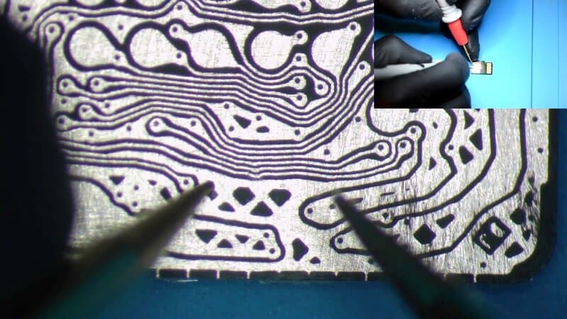
Exposed factory test pads on a decapsulated monolith. Each pad carries one NAND signal line the reader must map before the raw dump can start.
Reading the NAND is acquisition, not recovery. The raw dump is a fragmented, interleaved, XOR-scrambled binary matrix with no file system in it; the controller's live logical-to-physical map died with the controller.
Reassembly reverses the specific controller's handling of the data, which is closed, proprietary, & different for Phison, Silicon Motion, SanDisk, & Samsung parts. The dump goes through bad-column removal, then ECC correction & XOR descrambling in the order that controller requires. Most controllers compute ECC parity over the scrambled data, so ECC correction comes first; ACE Lab documents ITE, SSS, & AU controllers that need XOR descrambling applied first.
The last stage is page assembly: parsing each page's spare-area metadata, the logical sector numbers, block sequence numbers, & wear-level counters, to re-link the scattered pages into contiguous sectors. Only then does a mountable FAT32 or exFAT volume appear. A dedicated raw-NAND reader carries the maintained databases of XOR patterns, ECC schemes, & page formats that make this deterministic; a bare programmer dump does not.
The full page-assembly & retention-loss walkthrough lives on our monolithic microSD extraction page.
Chip-off recovers plaintext only when the data on the NAND is not hardware-encrypted. On a device with always-on hardware encryption, such as Apple T2 & Apple silicon Macs, a raw NAND read returns pure ciphertext. Desoldering the memory there accomplishes nothing.
The reason is where the key lives. On these devices the media key is generated & wrapped inside the controller or Secure Enclave & never leaves that silicon. The NAND stores high-entropy ciphertext that is indistinguishable from noise without the key, & transplanting the chip to a donor board fails because the donor presents a different key.
Most consumer USB sticks & SD cards are the opposite case: their data is only XOR-scrambled for electrical stability, not encrypted, so a raw read plus descrambling returns plaintext. Between those two extremes sit modern SSDs, where hardware AES is a per-drive fact, not a universal one; the exact controller decides whether a raw read is worth attempting.
When storage is genuinely encrypted & the host processor is dead, the only path to the data is board-level microsoldering to revive the original controller so it can decrypt its own payload. That is repair work, not extraction, & we tell you which case yours is before any paid work begins.
Flash & SD recovery runs $200–$1,500 across 4 tiers. Physical NAND extraction is the top tier, the chip-off tier at $1,200–$1,500, because it is the most involved & carries the reconstruction work; it takes a 50% deposit since decapsulation & desoldering are destructive to the package. A device that only needs board-level repair or file-system work sits in the lower tiers, From $200.
There is no diagnostic fee, & no charge if the data is unrecoverable.
Low complexity
Your flash drive or SD card works, you just need the data moved off it
Functional media; data transfer to new storage
Rush available: +$100
$200
3-5 business days
Low complexity
Most Common
Your flash drive or SD card isn't showing up, but it's not physically damaged
File system corruption. Visible to recovery software (R-Studio, UFS) but not to OS
Starting price; final depends on complexity
$300–$600
2-4 weeks
Medium complexity
Your flash drive or SD card has shorted components or won't power on
PCB issues: simple shorts, failed components on the drive's circuit board
May require a donor drive (additional cost)
$600–$900
3-6 weeks
High complexity
Your flash drive or SD card needs physical NAND chip extraction to recover the data
NAND chip extraction via soldering, pin-out identification, and raw data reconstruction
50% deposit required
50% deposit required
$1,200–$1,500
4-8 weeks
Our "no data, no fee" policy applies to hardware recovery. We do not bill for unsuccessful physical repairs. If we replace a hard drive read/write head assembly or repair a liquid-damaged logic board to a bootable state, the hardware repair is complete and standard rates apply. If data remains inaccessible due to user-configured software locks, a forgotten passcode, or a remote wipe command, the physical repair is still billable. We cannot bypass user encryption or activation locks.
No data, no fee. Free evaluation and firm quote before any paid work. Full guarantee details. Chip-off recovery requires a 50% deposit because the extraction process is destructive to the original media.
All prices are plus applicable tax.
Chip-off recovery reads a flash device's NAND memory directly, without routing through the device's own controller. On a discrete package the NAND chip is desoldered from the board and read in a socket. On a monolithic card the NAND and controller are separate dies wire-bonded inside one epoxy block, so the die is abraded open and read through its factory test pads instead. The raw dump that comes off either path is then reconstructed in software.
No, because a microSD has no separate memory chip to remove. It is a monolith: the NAND die and controller die are wire-bonded together and sealed in one epoxy Chip-on-Board package. There is nothing to unsolder. Reading it means abrading the epoxy to expose the factory test pads on the die substrate, then bonding micro-probes to the raw NAND bus. Discrete desoldering applies to full-size USB sticks and SSDs that carry a separate TSOP-48 or BGA NAND package.
Trapped moisture. Flash packages absorb humidity from the air, and when hot-air rework heats the package past the boiling point of water faster than the moisture can escape, the water flashes to steam inside the epoxy and delaminates or fractures the die. This is the popcorn effect that JEDEC J-STD-020 exists to prevent. A moisture-sensitive package gets baked dry before any heat, and bottom-side preheat brings the whole board to a steady temperature so the die never sees a sharp thermal gradient.
No. A cheap programmer can pull a bit-perfect dump off an unencrypted NAND die, but that dump is a fragmented, interleaved, XOR-scrambled binary matrix with no file system in it. Turning it into files requires reversing the specific controller's bad-column mapping, ECC scheme, XOR polynomial, and page assembly. That reconstruction is what a NAND reader with maintained controller databases provides, and what a raw programmer cannot.
No, not on its own. When storage is hardware-encrypted with a key bound to the host processor, as it is on Apple T2 and Apple silicon Macs and on SSD controllers running always-on AES, a raw NAND read returns only ciphertext. The decryption key never leaves that processor. The only path is board-level microsoldering to revive the original controller so it can decrypt its own data; desoldering the NAND accomplishes nothing.
Our Austin lab operates on a transparency-first model. We use industry-standard recovery tools, including PC-3000 and DeepSpar, combined with strict environmental controls to maintain drive integrity. This approach allows us to serve clients nationwide with consistent technical standards.
Open-drive work is performed in a ULPA-filtered laminar-flow bench, validated to 0.02 µm particle count, verified using TSI P-Trak instrumentation.
Serving clients nationwide via mail-in service since 2008. Our lead engineer holds PC-3000 and HEX Akademia certifications for hard drive firmware repair and mechanical recovery.
Our repair work has been covered by The Wall Street Journal and Business Insider, with CBC News reporting on our pricing transparency. Louis Rossmann has testified in Right to Repair hearings in multiple states and founded the Repair Preservation Group.
Our "No Data, No Charge" policy means we assume the risk of the recovery attempt, not the client.
Louis Rossmann
Our engineers review all lab protocols to maintain technical accuracy and honest service. Since 2008, his focus has been on clear technical communication and accurate diagnostics rather than sales-driven explanations.
We believe in proving standards rather than just stating them. We use TSI P-Trak instrumentation to verify that clean-air benchmarks are met before any drive is opened.
See our clean bench validation data and particle test videoRelated services
Trace-repair vs test-pad NAND read on the smallest monolith form factor
NAND pinout reference: D0-D7, CE/CLE/ALE/WE/RE/WP/R-B signal map
Desoldered NAND reads on solid-state drives
Dead USB sticks: controller repair and chip-off
Full-size SD, SDHC, SDXC cards
View complete catalog
Free evaluation. Firm quote before any work. No data recovered, no charge. Discrete chip-off, monolith test-pad extraction, and raw-NAND reconstruction, in-house at our Austin, TX lab.
